


An organic light-emitting diode (OLED) is a luminescent, thin-film component made of organic semi-conductive materials. As no silicon chips are needed, only pigment molecules, these lights can be produced with special ink jet or offset printers. They are cheaper, thinner and more flexible than LED lights, but their lifespan is shorter yet. Credit: Swiss Federal Laboratories for Materials Science and Technology
Organic light-emitting diodes (OLEDs) are the light sources of the future. Luminescent paintwork on cars, colorful living room walls and kitchen ceilings that light up, billboards of a very different kind – all this will now be conceivable. Last year the EU project TREASORES, coordinated by Empa, created flexible, transparent electrodes, the basis for supple, rollable OLEDs. Acquiring the experience to fabricate and functionalize the multi-layered structures of OLEDs light sources is the next step forward. After all, manufacturing a homogenously lit wallpaper is anything but trivial. Thus, expertise from the industry is urgently called for.
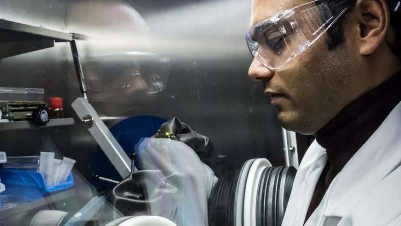
Anand Verma brings these expertise and know-how to the table. He started his career as a professional conventional printer at India Today after obtaining a Bachelor of Engineering in printing and media technology from Manipal Insititute of Technology. He extended his knowledge to the developing field of printed electronics by gaining a Master's degree at Chemnitz University of Technology (Germany). With his extensive research work on OLEDs in cooperation with Holst Center in Eindhoven (Netherlands), Novaled (Germany) and Cynora GmbH (Germany), he gained expertise to develop inks and new printing processes for OLED fabrication.
At Empa, as a coating / printing expert his area of research involves developing wet coating and printing for the Coating Competence Center (CCC). At CCC, he works on printing perovskite solar cells, actuators, and the like. Besides, he continues to explore the printing of flexible OLEDs on various substrates. "I can estimate optimal layer architectures, which will function in OLEDs depending on the substrates being investigated," says Verma. "So I also know the process parameters that need to optimized besides ink composition."
Ultrathin layers
Most of the light sources we are familiar with are point light sources or neon tubes. OLEDs, on the other hand, are surface lights. "If you look at OLED structure," explains the Empa researcher, "they consist of multiple nanometer-thin layers." The positively charged anode usually consists of transparent indium tin oxide (ITO), which can be used to produce electrically conductive windows or films. This is followed by an organic semiconductor layer (poly 3, 4-ethylenedioxythiophene polystyrenesulfonate, PEDOT:PSS), a light emitting layer (Super Yellow, fluorescent color), calcium for work function and a cathode, usually made of aluminum.
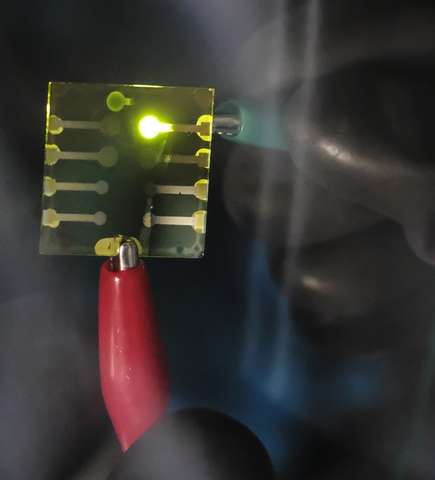
Credit: Swiss Federal Laboratories for Materials Science and Technology
Plasma makes for a smooth color
After the cleaning phase, the substrate is treated with an oxygen plasma: it is bombarded with ions to increase the surface energy, which facilitates wetting behavior of inks thus obtaining a homogeneous layer. It is important for the substrate's surface energy to be higher than that of the ink being coated. "Depending on the surface energy of the material and surface tension of the ink, it either wets the surface or it de-wets it. However, in some cases treating the substrate is not enough. When producing the ink – for the next layer of material – Verma first has to work out the right solvent in the ideal concentration to achieve the desired surface energy level, required thickness and morphology. Moreover, the solvent should be as environmentally friendly as possible. "If we chose chloroform, for instance," says Verma, "this would have a harmful impact on health during the production phase because rather high quantities of it are required." One of the used inks is Super Yellow. The most important layer is the light-emitting one. It is crucial for the researcher to already make this ink 24 hours beforehand as it takes that long for the solvent to dissolve in the dye. In contrast to the previous layers, calcium and subsequently aluminum is vacuum evaporated. To do so, the printing specialist has to use a glove box including a vacuum chamber to prevent the oxidation of calcium. Why opt for such a sensitive metal? "You could also use a different one. But all those that make suitable candidates are in the same group in the periodic table; they all oxidize."
Protected from oxygen and moisture
To use the fabricated devices in ambient conditions, Verma has to encapsulate the finished OLED to protect it from oxidation and moisture. This requires another layer made of transparent film or glass and special glue, which hardens under influence of UV light.
The tests involving the different substrates and the carriers for these flexible OLEDs will run until Empa's demonstrators light up reliably. Anand Verma is already thinking of the next step: "Printing and coating devices at Empa's new Coating Competence Center would already be capable of producing OLED patterns or surfaces on a larger scale." The lighting from the lab is within reach.